- 您现在的位置:买卖IC网 > Sheet目录1992 > DAC8562FP (Analog Devices Inc)IC DAC 12BIT PARALLEL 5V 20-DIP
REV. A
Information furnished by Analog Devices is believed to be accurate and
reliable. However, no responsibility is assumed by Analog Devices for its
use, nor for any infringements of patents or other rights of third parties
which may result from its use. No license is granted by implication or
otherwise under any patent or patent rights of Analog Devices.
a
+5 Volt, Parallel Input
Complete 12-Bit DAC
DAC8562
One Technology Way, P.O. Box 9106, Norwood, MA 02062-9106, U.S.A.
Tel: 617/329-4700
Fax: 617/326-8703
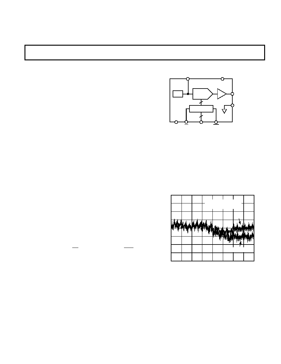
FUNCTIONAL BLOCK DIAGRAM
12-BIT
DAC
DAC REGISTER
REF
12
DATA
REFOUT
DGND
VOUT
AGND
VDD
CLR
CE
DAC-8562
GENERAL DESCRIPTION
The DAC8562 is a complete, parallel input, 12-bit, voltage out-
put DAC designed to operate from a single +5 volt supply. Built
using a CBCMOS process, these monolithic DACs offer the
user low cost, and ease-of-use in +5 volt only systems.
Included on the chip, in addition to the DAC, is a rail-to-rail
amplifier, latch and reference. The reference (REFOUT) is
trimmed to 2.5 volts, and the on-chip amplifier gains up the
DAC output to 4.095 volts full scale. The user needs only sup-
ply a +5 volt supply.
The DAC8562 is coded straight binary. The op amp output
swings from 0 to +4.095 volts for a one millivolt per bit resolu-
tion, and is capable of driving
±5 mA. Built using low tempera-
ture-coefficient silicon-chrome thin-film resistors, excellent
linearity error over temperature has been achieved as shown be-
low in the linearity error versus digital input code plot.
Digital interface is parallel and high speed to interface to the
fastest processors without wait states. The interface is very sim-
ple requiring only a single CE signal. An asynchronous CLR in-
put sets the output to zero scale.
The DAC8562 is available in two different 20-pin packages,
plastic DIP and SOL-20. Each part is fully specified for opera-
tion over –40
°C to +85°C, and the full +5 V ± 5% power supply
range.
For MIL-STD-883 applications, contact your local ADI sales
office for the DAC8562/883 data sheet which specifies opera-
tion over the –55
°C to +125°C temperature range.
1
–1
4096
–0.5
–0.75
0
–0.25
0.25
0.5
0.75
3072
2048
1024
VDD = +5V
TA = –55°C, +25°C, +125°C
LINEARITY
ERROR
—
LSB
DIGITAL INPUT CODE — Decimal
–55
°C
+25
°C & +125°C
Figure 1. Linearity Error vs. Digital Input Code Plot
FEATURES
Complete 12-Bit DAC
No External Components
Single +5 Volt Operation
1 mV/Bit with 4.095 V Full Scale
True Voltage Output,
5 mA Drive
Very Low Power –3 mW
APPLICATIONS
Digitally Controlled Calibration
Servo Controls
Process Control Equipment
PC Peripherals
发布紧急采购,3分钟左右您将得到回复。
相关PDF资料
DS1004Z-5+T
IC DELAY LINE 5TAP 25NS 8-SOIC
DS1005-125+
IC DELAY LINE 5TAP 125NS 14-DIP
DS1007S-2+T&R
IC DELAY LINE 4NS 16-SOIC
DS1010S-50+T&R
IC DELAY LINE 10TAP 16-SOIC
DS1013S-25+T&R
IC DELAY LINE 25NS 16-SOIC
DS1020S-50+T
IC DELAY LINE 256TAP 16-SOIC
DS1021S-50+T&R
IC DELAY LINE 256TAP 16-SOIC
DS1023S-25+W
IC DELAY LINE 256TAP 16-SOIC
相关代理商/技术参数
DAC8562FPZ
功能描述:IC DAC 12BIT PARALLEL 5V 20-DIP RoHS:是 类别:集成电路 (IC) >> 数据采集 - 数模转换器 系列:- 产品培训模块:Lead (SnPb) Finish for COTS
Obsolescence Mitigation Program 标准包装:50 系列:- 设置时间:4µs 位数:12 数据接口:串行 转换器数目:2 电压电源:单电源 功率耗散(最大):- 工作温度:-40°C ~ 85°C 安装类型:表面贴装 封装/外壳:8-TSSOP,8-MSOP(0.118",3.00mm 宽) 供应商设备封装:8-uMAX 包装:管件 输出数目和类型:2 电压,单极 采样率(每秒):* 产品目录页面:1398 (CN2011-ZH PDF)
DAC8562FR
制造商:未知厂家 制造商全称:未知厂家 功能描述:12-Bit Digital-to-Analog Converter
DAC8562FRU
功能描述:IC DAC 12BIT PARALLEL 5V 20TSSOP RoHS:否 类别:集成电路 (IC) >> 数据采集 - 数模转换器 系列:- 产品培训模块:Data Converter Fundamentals
DAC Architectures 标准包装:750 系列:- 设置时间:7µs 位数:16 数据接口:并联 转换器数目:1 电压电源:双 ± 功率耗散(最大):100mW 工作温度:0°C ~ 70°C 安装类型:表面贴装 封装/外壳:28-LCC(J 形引线) 供应商设备封装:28-PLCC(11.51x11.51) 包装:带卷 (TR) 输出数目和类型:1 电压,单极;1 电压,双极 采样率(每秒):143k
DAC8562FRU-REEL7
功能描述:IC DAC 12BIT PARALLEL 5V 20TSSOP RoHS:否 类别:集成电路 (IC) >> 数据采集 - 数模转换器 系列:- 产品培训模块:Data Converter Fundamentals
DAC Architectures 标准包装:750 系列:- 设置时间:7µs 位数:16 数据接口:并联 转换器数目:1 电压电源:双 ± 功率耗散(最大):100mW 工作温度:0°C ~ 70°C 安装类型:表面贴装 封装/外壳:28-LCC(J 形引线) 供应商设备封装:28-PLCC(11.51x11.51) 包装:带卷 (TR) 输出数目和类型:1 电压,单极;1 电压,双极 采样率(每秒):143k
DAC8562FRUZ
功能描述:IC DAC 12BIT PARALLEL 5V 20TSSOP RoHS:是 类别:集成电路 (IC) >> 数据采集 - 数模转换器 系列:- 产品培训模块:Data Converter Fundamentals
DAC Architectures 标准包装:750 系列:- 设置时间:7µs 位数:16 数据接口:并联 转换器数目:1 电压电源:双 ± 功率耗散(最大):100mW 工作温度:0°C ~ 70°C 安装类型:表面贴装 封装/外壳:28-LCC(J 形引线) 供应商设备封装:28-PLCC(11.51x11.51) 包装:带卷 (TR) 输出数目和类型:1 电压,单极;1 电压,双极 采样率(每秒):143k
DAC8562FS
功能描述:IC DAC 12BIT PARALLEL 5V 20-SOIC RoHS:否 类别:集成电路 (IC) >> 数据采集 - 数模转换器 系列:- 产品培训模块:Data Converter Fundamentals
DAC Architectures 标准包装:750 系列:- 设置时间:7µs 位数:16 数据接口:并联 转换器数目:1 电压电源:双 ± 功率耗散(最大):100mW 工作温度:0°C ~ 70°C 安装类型:表面贴装 封装/外壳:28-LCC(J 形引线) 供应商设备封装:28-PLCC(11.51x11.51) 包装:带卷 (TR) 输出数目和类型:1 电压,单极;1 电压,双极 采样率(每秒):143k
DAC8562FS-REEL
功能描述:IC DAC 12BIT PARALLEL 5V 20-SOIC RoHS:否 类别:集成电路 (IC) >> 数据采集 - 数模转换器 系列:- 产品培训模块:Data Converter Fundamentals
DAC Architectures 标准包装:750 系列:- 设置时间:7µs 位数:16 数据接口:并联 转换器数目:1 电压电源:双 ± 功率耗散(最大):100mW 工作温度:0°C ~ 70°C 安装类型:表面贴装 封装/外壳:28-LCC(J 形引线) 供应商设备封装:28-PLCC(11.51x11.51) 包装:带卷 (TR) 输出数目和类型:1 电压,单极;1 电压,双极 采样率(每秒):143k
DAC8562FSZ
功能描述:IC DAC 12BIT PARALLEL 5V 20SOIC RoHS:是 类别:集成电路 (IC) >> 数据采集 - 数模转换器 系列:- 标准包装:1 系列:- 设置时间:4.5µs 位数:12 数据接口:串行,SPI? 转换器数目:1 电压电源:单电源 功率耗散(最大):- 工作温度:-40°C ~ 125°C 安装类型:表面贴装 封装/外壳:8-SOIC(0.154",3.90mm 宽) 供应商设备封装:8-SOICN 包装:剪切带 (CT) 输出数目和类型:1 电压,单极;1 电压,双极 采样率(每秒):* 其它名称:MCP4921T-E/SNCTMCP4921T-E/SNRCTMCP4921T-E/SNRCT-ND